Table of Contents >> Show >> Hide
- Why DIY PCB Vias Are Such a Pain in the First Place
- How Commercial Via Plating Normally Works
- What “Without Chemical Baths” Really Means
- How the Home Method Works in Practice
- Why This Approach Is Genuinely Exciting
- The Catch: Physics Is Still in the Room
- Alternatives That Still Deserve Respect
- When This Technique Makes Sense
- The Real Verdict
- Experience Notes: What This Feels Like in a Real Home Workshop
If you have ever made a double-sided PCB at home, you already know the tiny villain in this story: the via. Traces are manageable. Drilling is annoying but survivable. Alignment is a character-building exercise. But getting a reliable electrical connection from one side of the board to the other without turning your workbench into a chemistry lab? That is where many brave makers suddenly start pricing board fab services instead.
And honestly, that reaction is fair. Commercial PCB shops make plated through-holes look effortless because they have industrial processes, controlled chemistry, and equipment that does not live next to your coffee mug. At home, the usual backup plan has been gloriously low-tech: jam a tiny wire through the hole, solder both sides, trim, repeat, and question your life choices around via number thirty-seven.
That is why the idea of electroplating DIY PCB vias at home without chemical baths is so interesting. It promises something that sits between the full-on industrial plating line and the caveman method of “wire, solder, snip, sigh.” The trick is not magic. It is more like clever compromise: create a conductive seed inside the hole, then use localized electroplating or selective plating methods so you do not need to dunk the whole board into a series of nasty baths just to connect a few layers.
Done right, this approach can make home PCB fabrication more elegant, more repeatable, and less messy. Done badly, it can leave you with flaky vias, inconsistent plating, and a board that passes continuity on Tuesday and betrays you by Thursday. Let’s walk through what this technique really means, why it matters, where it shines, and where old-school alternatives still deserve a standing ovation.
Why DIY PCB Vias Are Such a Pain in the First Place
A via is basically a tiny vertical tunnel that connects copper on one layer of a printed circuit board to copper on another. In professional manufacturing, that tunnel is copper-lined, which is why signals, ground, and sometimes heat can move through it reliably. In a home shop, once you drill a hole through FR-4, the inside wall is mostly non-conductive fiberglass and resin. That means electricity sees your lovingly drilled via wall and says, “Absolutely not.”
That is the whole problem. You can etch traces on the top and bottom of a board, but unless the inside of the hole becomes conductive, the two sides are still just neighbors with trust issues. That is why hobbyists traditionally rely on three workarounds: soldered wire links, through-hole component leads that act as accidental interconnects, or tiny copper eyelets and rivets. All of those methods can work. None of them are especially glamorous under a microscope.
For simple prototypes, those methods are fine. For denser layouts, small-pitch parts, or boards with lots of interlayer transitions, they get old fast. Wire vias are fiddly. Rivets need the right hole size, the right board thickness, and a decent setting technique. Component-lead stitching only helps where components happen to exist. In other words, the via problem keeps coming back like a sequel nobody asked for.
How Commercial Via Plating Normally Works
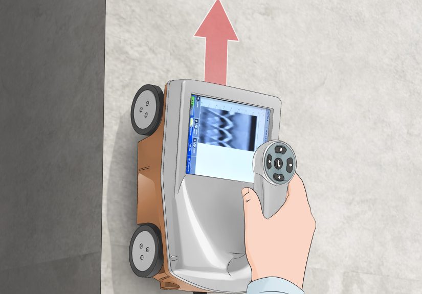
To understand the appeal of the no-bath approach, it helps to know what happens in a fab house. After drilling, the board typically goes through cleaning and desmear steps so the hole walls are ready to accept metal. Then comes the crucial part: a seed layer. In industrial PCB manufacturing, this is often created through electroless copper deposition after activation. That ultra-thin conductive layer makes the entire hole wall ready for the next step, which is electroplating more copper until the via barrel reaches a useful thickness.
That sequence matters because electroplating alone cannot build copper onto a non-conductive hole wall. The current needs somewhere to go first. No seed layer, no real plated through-hole. That is why the home-brew dream has always run into the same brick wall: the process is not just “apply electricity and believe in yourself.” You first need a way to make the inside of the hole conductive enough to start plating.
Professional shops also plate to meaningful thickness. In normal fabrication discussions, via wall copper is often described in the neighborhood of roughly 20 to 30 microns for through-plating, depending on specs and process targets. That is one reason commercial vias are so dependable. They are not dusted with copper like a pastry; they are built up with controlled, measurable metal.
What “Without Chemical Baths” Really Means
Here is the important reality check: without chemical baths does not mean “without chemistry.” Copper still does not teleport onto fiberglass because you asked nicely. What it usually means is avoiding the full series of immersion tanks used in conventional electroless copper processing and instead using a more targeted method.
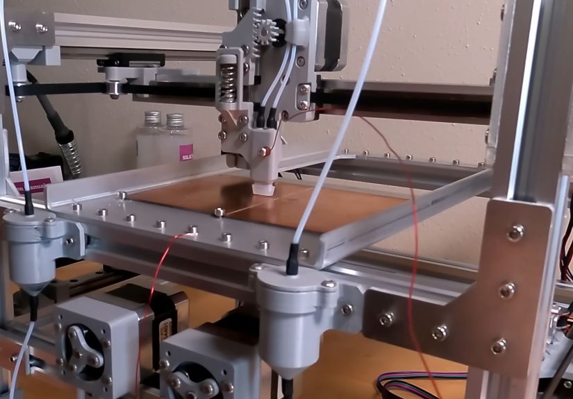
The modern DIY idea looks something like this: first, coat the drilled via wall with a conductive material, often a graphite- or carbon-based conductive ink. That creates a high-resistance but usable path. Next, use localized electroplating, brush plating, or a similarly selective method to deposit copper where you need it, without submerging the entire board in a large plating bath. Think of it less as swimming and more as sponge-bathing your vias. Not glamorous, but oddly efficient.
This is clever for two reasons. First, it reduces the need for specialty activation chemistry that is annoying to source and even more annoying to store. Second, it makes the process more suitable for small-scale prototyping, because you can focus effort only on the vias or exposed conductive areas that actually matter.
How the Home Method Works in Practice
1. Drill and clean the holes well
This part is boring, which is exactly why it matters. Burrs, resin smear, dust, and greasy fingerprints are the enemies of adhesion. If the via wall is dirty, the conductive coating will be inconsistent, and inconsistent is just a fancier word for “future debugging session.”
2. Add a conductive seed layer
In the home-shop version, this is often the breakthrough step. Instead of full electroless copper activation and deposition, the hole wall is coated with conductive ink or graphite paint. The goal is not to make the final conductor right away. The goal is to make the hole conductive enough that electroplating can start building real copper on top of it.
3. Make sure the seed actually connects to the copper pads
This is where many DIY attempts become science projects. The coating has to bridge the via wall to the copper annular ring reliably. If it does not make good contact, the plating current will not flow properly, and your via becomes more decorative than functional.
4. Plate selectively instead of dunking the whole board
Brush plating or other localized techniques allow copper deposition without immersing the whole PCB in a large tank. This is appealing for repair work, prototypes, and one-off boards. It is also a lot easier to justify in a small workshop where your ventilation plan should not involve “opening a window and hoping for the best.”
5. Inspect, test, and then test again because optimism is not a measurement tool
Continuity testing is the minimum. Mechanical reliability matters too. A via that works until the first reheating cycle is not a triumph; it is a practical joke. For prototype use, low-current signal paths are the safest place to trust new DIY via methods first.
Why This Approach Is Genuinely Exciting
The best thing about this method is that it tries to preserve the logic of real PCB manufacturing while stripping away the messiest part for hobbyists. Instead of pretending wire links are the future, it says: what if we could still seed the hole wall, still plate copper, and still get a true conductive barrel, just with a much smaller, more accessible setup?
That has real advantages. It can reduce hand-soldered via clutter. It can make boards easier to assemble. It can help with denser layouts where traditional wire-through methods become awkward. It may also be more automatable than manual rivets or little U-shaped wire tricks, which is why recent projects around this idea have attracted so much attention.
There is also a philosophical appeal here. Good DIY engineering is rarely about copying a factory step for step. It is about finding the smallest workable version of a factory process and making it behave on a kitchen-table budget. That is exactly what selective via electroplating is trying to do.
The Catch: Physics Is Still in the Room
Now for the less romantic part. This method is promising, but it is not yet a miracle cure for every garage-built PCB. One of the big issues is speed. Recent no-bath experiments have shown that plating a single small via can still take several minutes, and for very small vias the process can become painfully slow. If your design has only a handful of vias, that may be fine. If your board looks like a cheese grater, you may want to sit down before doing the math.
Another issue is uniformity. A conductive ink seed layer is not the same as a professionally activated, chemically deposited copper layer. The resistance can be higher, the coverage can vary, and the resulting plating may not build as evenly along the full hole wall. That does not automatically make it useless, but it does make it less predictable.
Then there is current handling. A DIY plated via that works beautifully for a signal line is not automatically ready to carry serious power or thermal load. Via reliability depends on plating thickness, hole geometry, adhesion, and total cross-sectional copper area. In other words, the words “it beeped on my multimeter” should not immediately become “therefore it is production-ready.”
Alternatives That Still Deserve Respect
Wire vias
The oldest DIY solution remains one of the most dependable. Thread a small wire through the hole, solder both sides, trim it close, and move on. It is not pretty. It is not fast. But it is cheap, understandable, and mechanically solid when done well.
Via rivets or eyelets
These are a surprisingly elegant middle ground. Tiny copper eyelets can create a neat plated-through look and reduce some of the hand-solder mess. They still demand correct sizing and a steady technique, but they are often a better option than people expect for repeatable home prototypes.
Component-lead stitching
When a through-hole part already spans the board, soldering both sides can eliminate the need for a dedicated via nearby. It is not universally applicable, but it is one of those wonderfully pragmatic tricks that makes a layout feel smarter than it actually is.
When This Technique Makes Sense
Electroplating DIY PCB vias at home without chemical baths makes the most sense when you are building low-volume prototypes, experimenting with process development, or trying to automate a cleaner home fabrication workflow. It is especially interesting if you hate the chemical overhead of traditional through-hole plating but still want something more elegant than stuffing bits of wire into every interconnect.
It makes less sense when you need a lot of tiny vias, tight consistency, high current capability, or production-grade repeatability. At that point, sending the board to a professional fab is usually the more rational move. There is no shame in that. Outsourcing a solved problem is not failure. It is time management wearing safety glasses.
The Real Verdict
The no-bath via-plating idea is neither fantasy nor finished revolution. It sits in that delicious engineering middle zone where the concept is sound, the early results are promising, and the workflow is still rough around the edges. That is usually where the fun lives.
For hobbyists and prototype builders, the important lesson is not that chemical-bath-free via plating has completely replaced wire links or rivets. It has not. The lesson is that the barrier to making plated through holes at home is getting lower. Conductive inks, selective plating, and smarter localized processes are turning what used to be a full chemistry problem into more of a precision process problem. That is progress.
So yes, you can get closer to real electroplated vias at home without building a mini PCB factory in your garage. Just go in with clear expectations. This is a method for careful prototypes and process nerds, not a magic shortcut to factory-grade boards on your first Saturday afternoon. Still, for the right project, that tiny copper-lined hole can feel like a very big win.
Experience Notes: What This Feels Like in a Real Home Workshop
The lived experience around this topic tends to follow the same emotional arc, and it is oddly comforting. First comes excitement. You discover that someone has found a way to make DIY PCB vias more “real” without the full industrial parade of activation tanks, formal chemistry, and permanent bench stains. Suddenly, the dream seems close enough to touch. You imagine clean, copper-lined holes, tidy two-layer boards, and a workbench that does not look like a hazardous-waste field trip.
Then comes the first reality check: the process is much more sensitive than it sounds in a headline. Tiny differences in hole cleanliness, conductive ink coverage, pad contact, and plating time matter a lot. Hobbyists often report that the first few attempts are not catastrophic so much as confusing. One via works perfectly, the next is intermittent, and the third behaves like it has entered a witness protection program. This is the stage where you realize that “repeatable” and “possible” are cousins, not twins.
There is also the strange psychological effect of working at via scale. A PCB trace feels visible. A pad feels tangible. A via wall feels like an argument with dust. You spend an absurd amount of attention on holes so small that a non-engineer would assume you had lost the plot. And yet, when one of those tiny plated holes finally tests correctly and survives soldering, the satisfaction is wildly out of proportion to its size. You do not just feel like you made a connection. You feel like you bullied materials science into cooperating.
Another common experience is discovering that workflow matters more than heroics. The builders who seem happiest are not the ones improvising every step from memory like kitchen alchemists. They are the ones who standardize things: drill size, board thickness, cleaning routine, coating method, plating time, inspection habit. Once a method becomes consistent, the stress level drops. The project stops feeling like a dramatic experiment and starts feeling like a process.
And then, eventually, comes the most useful realization of all: not every board deserves this treatment. That sounds less romantic, but it is actually empowering. Some designs really do benefit from this approach, especially small prototype runs where a handful of vias can be plated carefully. Other designs are better served by wire vias, copper rivets, or simply sending Gerbers to a fab house and using the waiting time to do literally anything else productive. The most experienced DIY builders tend to land there. They do not worship one method. They keep options on the bench and choose the one that fits the job, the risk, and the number of tiny holes trying to ruin the evening.